Artificial Intelligence, automated driving and the Internet of Things (IoT) are gaining popularity. That places huge demands on devices and data centers to process higher volumes of information more quickly than ever. And it requires rapid advances in high-performance, safe and sustainable computer chips. Henkel’s innovative portfolio is supporting this digital revolution by enabling larger, more reliable semiconductors.
Success Story
High-tech underfill solutions open up new design possibilities for computer chips

Short on time? Dive into the key chapter of your interest:
Cell phones are acting as personal assistants and cars are taking over the steering wheel. Artificial Intelligence (AI) is transforming every aspect of modern life right now. Companies are adding functions to products across categories. That creates big challenges for data centers and computer chips that store and process this mountain of digital information.
One possible solution is to make computer chips bigger. Large semiconductor die packages, as they are known, offer potential to expand capacity for high-performance computing (HPC). However, producing and operating large die packages involves complex applications that require advanced solutions to protect silicon materials against heat, stress and other damage.
Safe and sustainable innovations from Henkel are ensuring next-level performance and durability for large die packages. Find out how…

Our fast-flow and highly reliable underfill solutions put us in a strong position to meet demands for larger packages.
Arsia Khanfekr, Sr. Engineer, Application Engineering Semiconductor, Henkel Adhesive Technologies

We work closely with leaders in this industry to unlock next-generation technologies together.
Raj Peddi, Market Strategy Manager Semiconductor, Henkel Adhesive Technologies

Henkel’s portfolio features innovations that support progress for every application involved in creating durable large die designs.
Chunlin He, Sr. Scientific Associate, Product Development Encapsulation, Henkel Adhesive Technologies
1 of 3
Excellence for electronics
Digital devices are often small – but contain a vast number of complex and specialized technologies. That includes materials that facilitate the flow of electricity to components, strengthen the structure of the device or manage heat in small spaces. It also involves advanced formulations that improve safety or help to reduce greenhouse gas emissions.
Henkel offers a unique portfolio of solutions for the electronics industry. Its teams also share their expertise to help big-name customers in this market to unlock new designs, boost performance and stay ahead of regulatory expectations. The company’s products include Thermal Interface Materials (TIMs), underfill technologies, Liquid Compression Molding (LCM) and lid or stiffener attach adhesives. And Henkel is also a leading provider of materials for semiconductor packaging.
>$69 billion
is the predicted market revenue from advanced die packaging by 2029.
30 %
faster is the rate at which Henkel's underfills fill gaps in semiconductor chips compared to previous-generation products.
>10
times larger is the expected increase in die package designs in the next few years.
Supersizing semiconductors
A semiconductor is a material, usually silicon, that is used to control the flow of electricity within an electronic component. This piece of silicon is also known as a die. It contains integrated circuits that define how the component will function within a device. These materials are encased in a protective shell made of plastic, called a package. Metal pins or legs then connect the component to other electronic parts.
Today’s typical die packages for cell phones, tablets or laptops are about 10-square millimeters in size. However, manufacturers are responding to the rise of AI, HPC and the IoT by exploring new designs for larger die packages that are ten times bigger. In this way, they aim to grab a competitive advantage by enabling devices and data centers to meet shifting requirements – while also ensuring reliability and sustainability.

Outperforming underfills
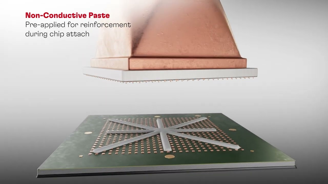
Innovative semiconductor underfill technologies from Henkel are supporting this switch to larger die package architectures. Henkel’s LOCTITE® ECCOBOND UF 9000AE provides robust protection and enables efficiency improvements during manufacturing. These epoxy-based liquids are applied between the semiconductor and its package. By filling gaps in this tiny space, they protect the chip from damage caused by heat or physical impacts.
Importantly, these solutions use capillary motion to fill tiny gaps. This motion results from intermolecular forces between liquids and surrounding solid surfaces. In this way, the underfill is distributed evenly and quickly without assistance from external forces like gravity. Henkel’s underfills are 30 percent faster than previous-generation technologies in mass-production. They have also proven their performance in testing that involved exposure to cycles of extreme temperature – from minus 65 degrees Celsius up to 150 degrees Celsius.
Experts from Henkel regularly visit industry-leading computer chip manufacturers to understand their specific challenges and develop solutions together. Recently, specialists from Henkel helped a major player in this market to design a new dispensing approach that ensures a thin Keep-out-zone (KOZ) – so no overflow of material runs over the edge of the package. Several further customers have now qualified and approved this new approach for their processes.
LOCTITE® underfill solutions
Turbo-charged testing
In such a cutting-edge and fast-moving industry, it is essential for partners to collaborate and share expertise. That is why Henkel operates a global network of innovation and application centers, while also leveraging digital tools to help customers bring new semiconductor designs to market faster, more sustainably and more competitively.
Henkel’s virtual modelling approach makes it possible to simulate physical testing and evaluate potential products faster than ever. By shrinking this step in the development process, Henkel enables customers to identify next-generation formulations and designs with just a few mouse clicks – saving time and energy, while also accelerating time-to-market.
Fast, flexible and future-ready
The digital revolution is not a novel trend but it is entering a new phase that puts huge demands on components, devices and data centers. Semiconductor manufacturers have an opportunity to move ahead of competitors by delivering safe, sustainable and high-performance large die packages that support the transition to a data-driven future.
At Henkel, our portfolio for the electronics industry is truly comprehensive – and expanding all the time. Technical specialists in our laboratories are pushing the boundaries of what is possible for large die packaging. As these small components grow in size, flexible and advanced technologies from Henkel are enabling innovative designs that meet demand for faster and more reliable data processing. And our experts are constantly creating more solutions to unlock next-level performance and durability.

Visit our Global
Innovation Centers
Gain hands-on experience with our latest innovations. Our experts will guide you through our cutting-edge technologies and help you develop customized solutions that meet your specific needs.


1 of 4
OUR SOLUTIONS


EXPLORE HOW
WE MAKE IT HAPPEN
Discover more about how we drive innovation and sustainability and explore even more success stories on the megatrends that inspire us.
MORE ABOUT
ADHESIVE TECHNOLOGIES
Discover the brand portfolio of our Adhesive Technologies business and learn more about the industries we operate in.